Etching your own PCB’s in a classroom
A couple of years ago, one of my former students came to visit. He brought business cards and a selection of little printed circuit-boards, or PCB’s. My questioning turned into a lesson in which a 15-year-old kid taught me how to install some circuit-designing software, create my own circuit board, export the design and e-mail it to a factory in China where the boards would be manufactured and mailed to me. It was one of the most empowering things I’ve ever learned! I feel I got some valuable consulting work from this student, and he provided it for free. What a generous gift and a valuable example of a teacher and student learning together.
A former student taught me how to make this!
I found out since that time that you can actually etch your own printed circuit boards at home, for quick prototyping. In electronics class, my co-worker Tracey and I created an engineering project for the students: design or modify a small, rechargeable LED-based lantern that works. This semester, I thought I would offer the opportunity for students to learn to etch their own PCB’s if they wanted to do it for their design. This was a rich and challenging project, and I want to share how we did this with middle school kids – with some notes of caution. It’s hard to do in a big group. I was grateful to have Tracey’s presence to work with most of the class on an alternate lesson while I took small groups to work on PCB design and etching. It was failure-prone and high-frustration, but also high-reward. Here’s how we did it.
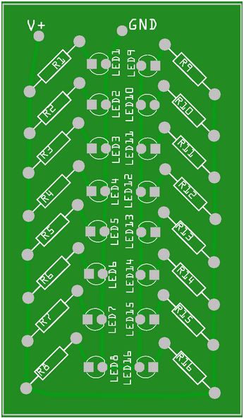
First, the students need to design their circuit and generate a high quality, printable image of the copper traces. I used Fritzing, a free program that is fairly easy to use. I taught the students how to lay out a simple parallel circuit with resistors and LED’s. The components can be either surface mount (SMD) or through-hole (THT), but you want to choose Through-hole. Pay attention to the pin spacing to make sure it matches the components you have. In our case, we needed 3 mm spacing for the LED’s and 400 mils (these are thousandths of an inch, not the same as mm) for the resistors. I don’t know why the default units were different. I added a couple of via’s to connect to the switch and battery. Choose the “home-etched” setting for via’s to make them a little bigger.
Completed simple PCB in Fritzing. Most students added 5 or 6 resistor/LED pairs.
Students could add as many resistor/LED pairs as they wanted, and rearrange them as needed. Some students created some interesting layouts for their PCB.
Next, we had to export the file to a high quality PDF. In Fritzing, choose File –> Export –> As Image –> PDF.
I stitched together a couple of methods from online articles for the etching part. This article from Hackaday used the magazine page transfer method, and it worked all right with some cautions.
Here are the supplies you need for this step..
- Glossy magazine paper and a laser printer. We found the alumni magazine from my university works well! Its 8 1/2 by 11 size and nice sturdy paper loaded and printed in the laser printer perfectly. We had some success with catalogs pulled from my mailbox too, although the paper was thinner so it tended to jam.
- One-sided copper clad PCB. You can get lots of this very cheap on eBay.
- An iron and ironing board (we borrowed these from the family consumer science teacher)
- A scotch-brite scrubbing pad.
You need to load the glossy paper into your laser printer and print the PDF of the copper traces. Fritzing will export a lot of files into a folder – print the one that ends in “copper_top_mirror”. You might have to try a few times before you get a nice printout on the magazine paper.
Buff the copper-clad PCB with the scotch-brite pad, until it’s roughed up a little.
Turn the iron to its hottest setting, and make sure there’s no water in the iron. Put the magazine paper with the image on it face-down onto the copper clad. Push down HARD with the iron for a full two minutes. Then move the iron around still pressing down hard, for 4 more minutes. This process sometimes took 4 tries to get a good transfer and was really difficult with a number of groups to work with. Imagine it takes pressure on every wire trace in order to transfer it from the paper to the board, and visualize how you have to press the iron down to make this happen.
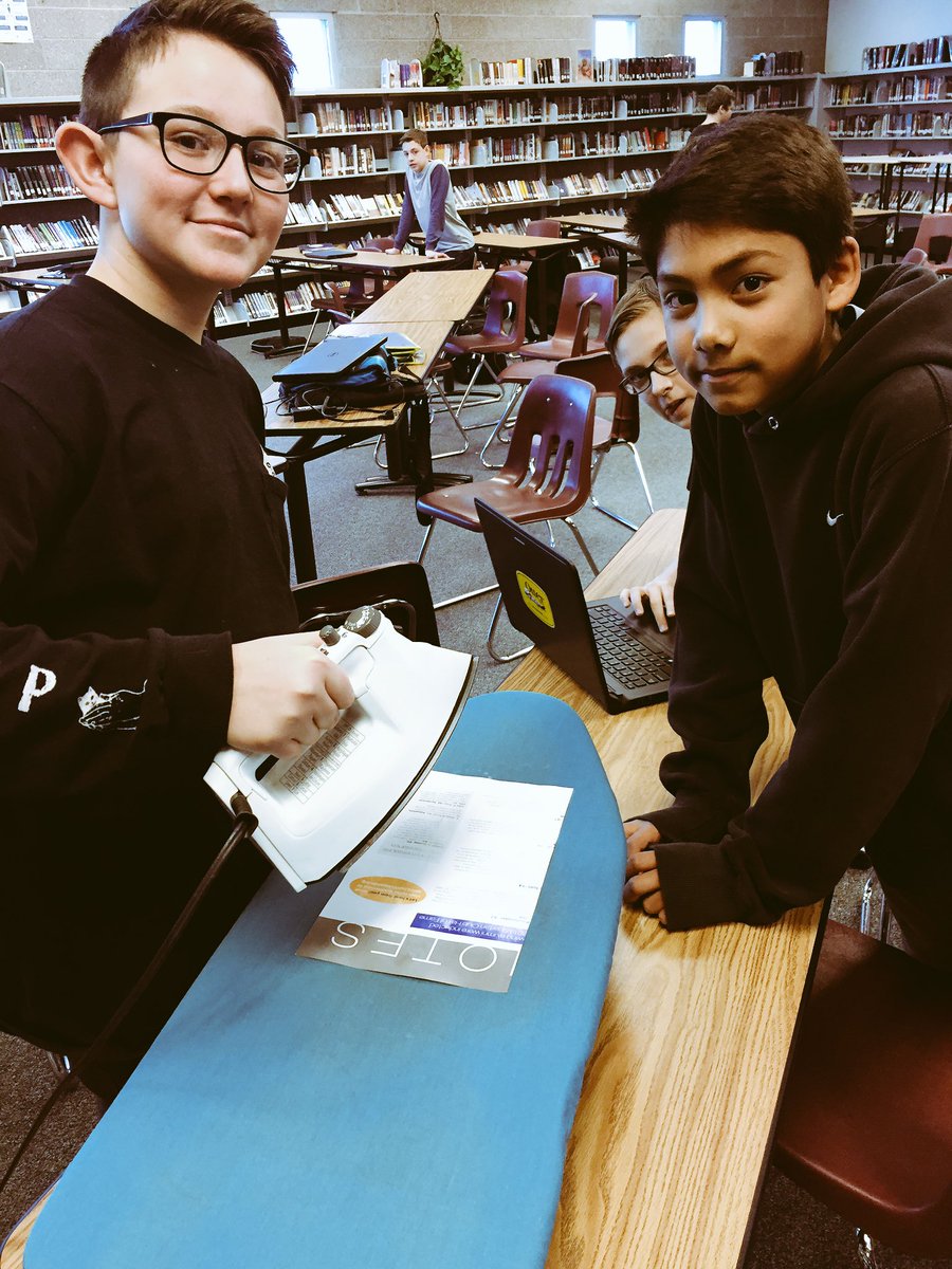
Ironing. For the first time ever.
Inspect the copper clad to make sure the image transferred with no thin or broken spots. We attempted to fix a couple of the designs with Sharpie, but it really didn’t work well. Better to transfer properly the first time.
A bad transfer, and a better one.
Now you’re ready for the etching. For this part, I used the second half of the instructions from Blondihack. Some blogs recommend using muriatic acid, but with middle-schoolers the normal kitchen chemicals are the way to go here. You will not regret using plain old vinegar. You really should use a proper science lab with fume hoods, sinks and safety equipment. At the very least, make sure you have safety goggles and nitrile gloves for everyone, and access to a sink. To do the etching, you need:
- White vinegar
- Household hydrogen peroxide
- Some salt
- Foam brushes
- Plastic tubs
- Measuring cups and spoons
- Safety goggles and gloves
- A timer
- Acetone (nail polish remover)
It’s pretty simple. Pour equal portions of hydrogen peroxide and vinegar into a shallow plastic tub. Add about a teaspoon of salt and stir it gently. When the salt is dissolved, put the PCB into the solution. You’ll see a film of yellowish gunk appear on the board, and over time the liquid will turn blue. About once a minute, use the foam brush to wipe the gunk off. It took us about 50 minutes to complete the etching. When you’re close to done, the edges of your board will be free of copper. You’ll know you’re done when all of the copper is dissolved except for what’s under the black toner. When you’re at this point, rinse the board with lots of water. We washed the remaining etching solution down the drain with lots and lots of fresh water.
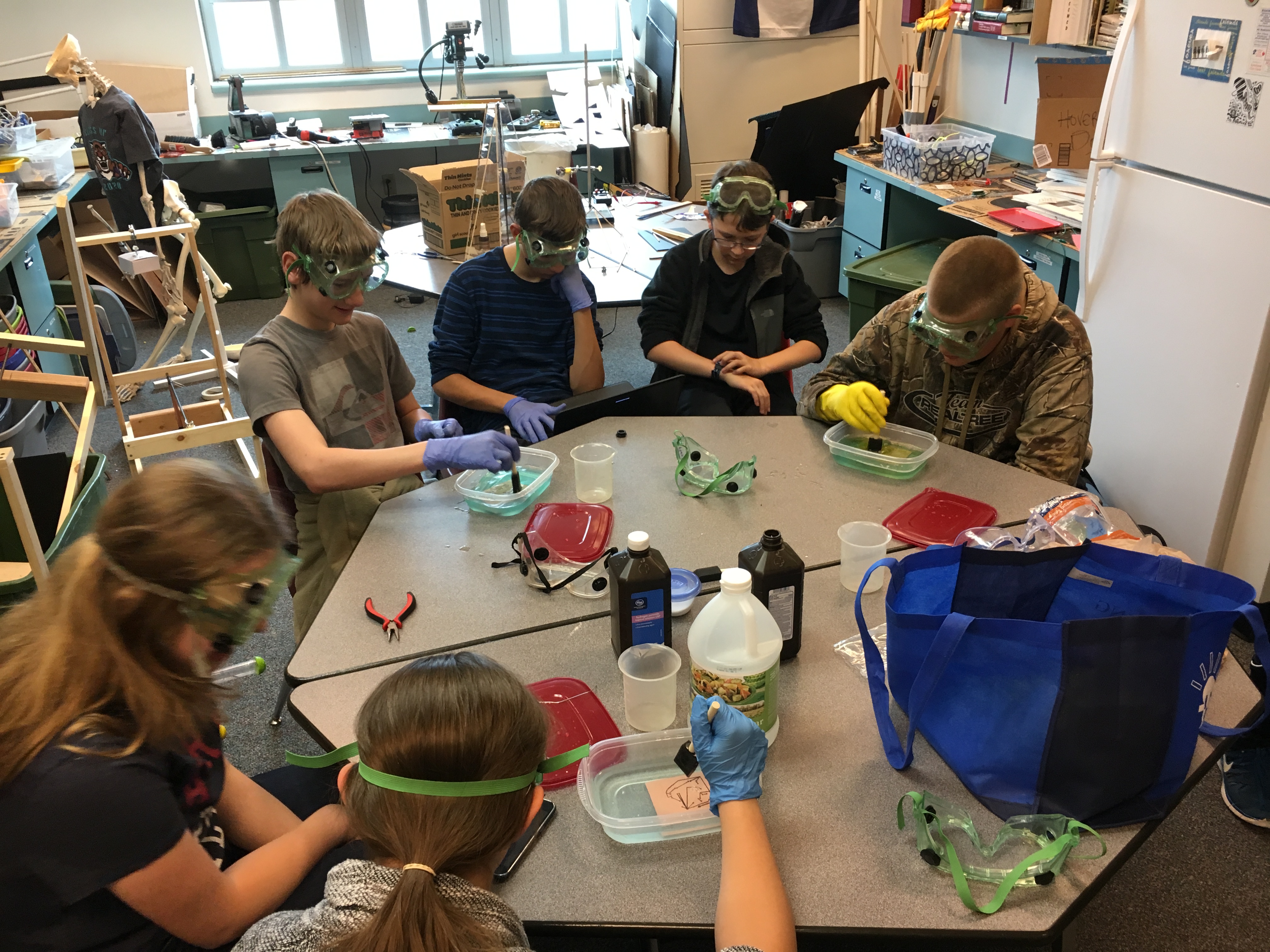
This is boring work, but the kids don’t mind socializing while they wipe the boards down once a minute.
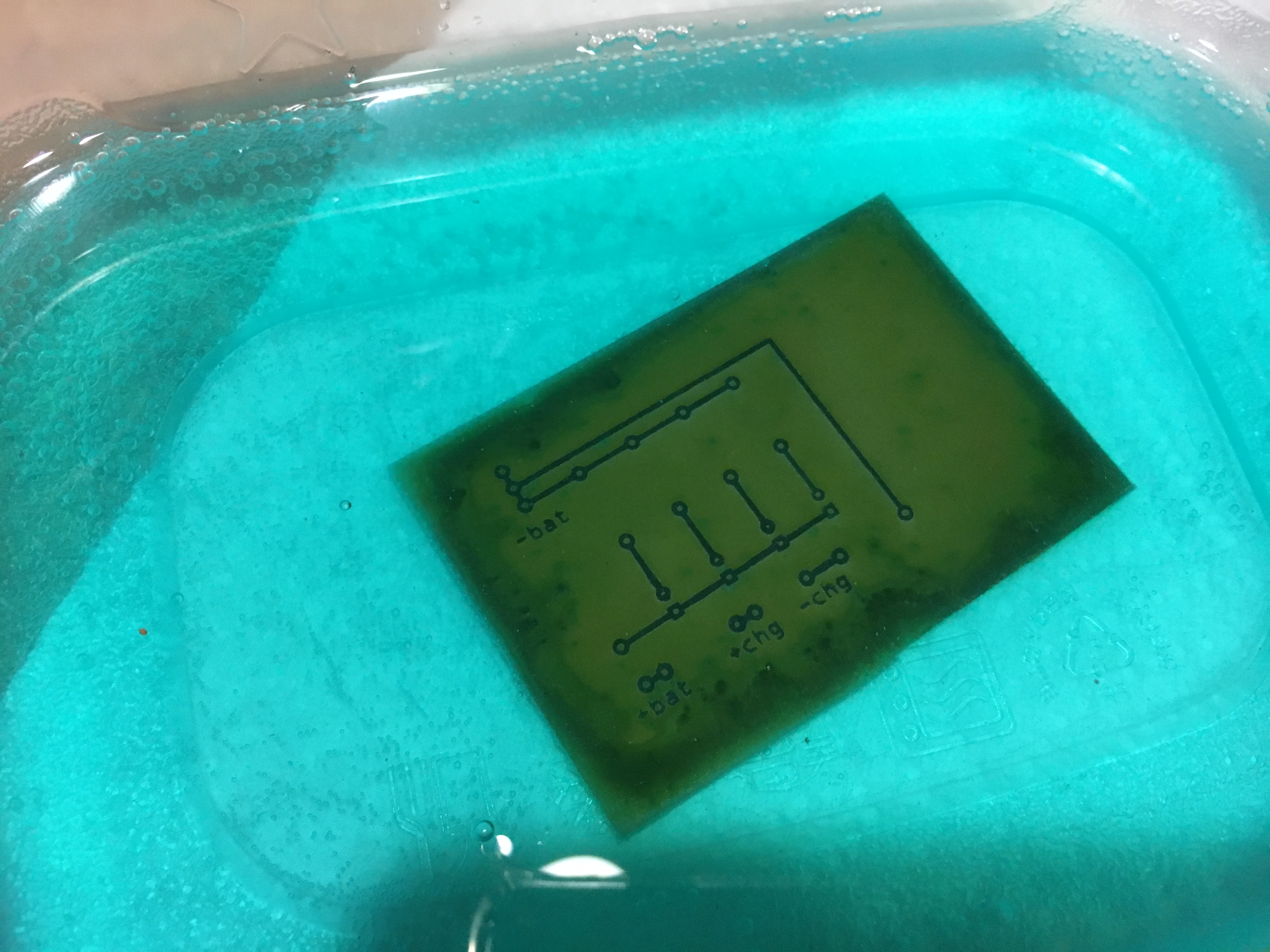
When you’re close to done, you can see the edges of the board are free of copper.
Done, rinsed and ready for the next step.
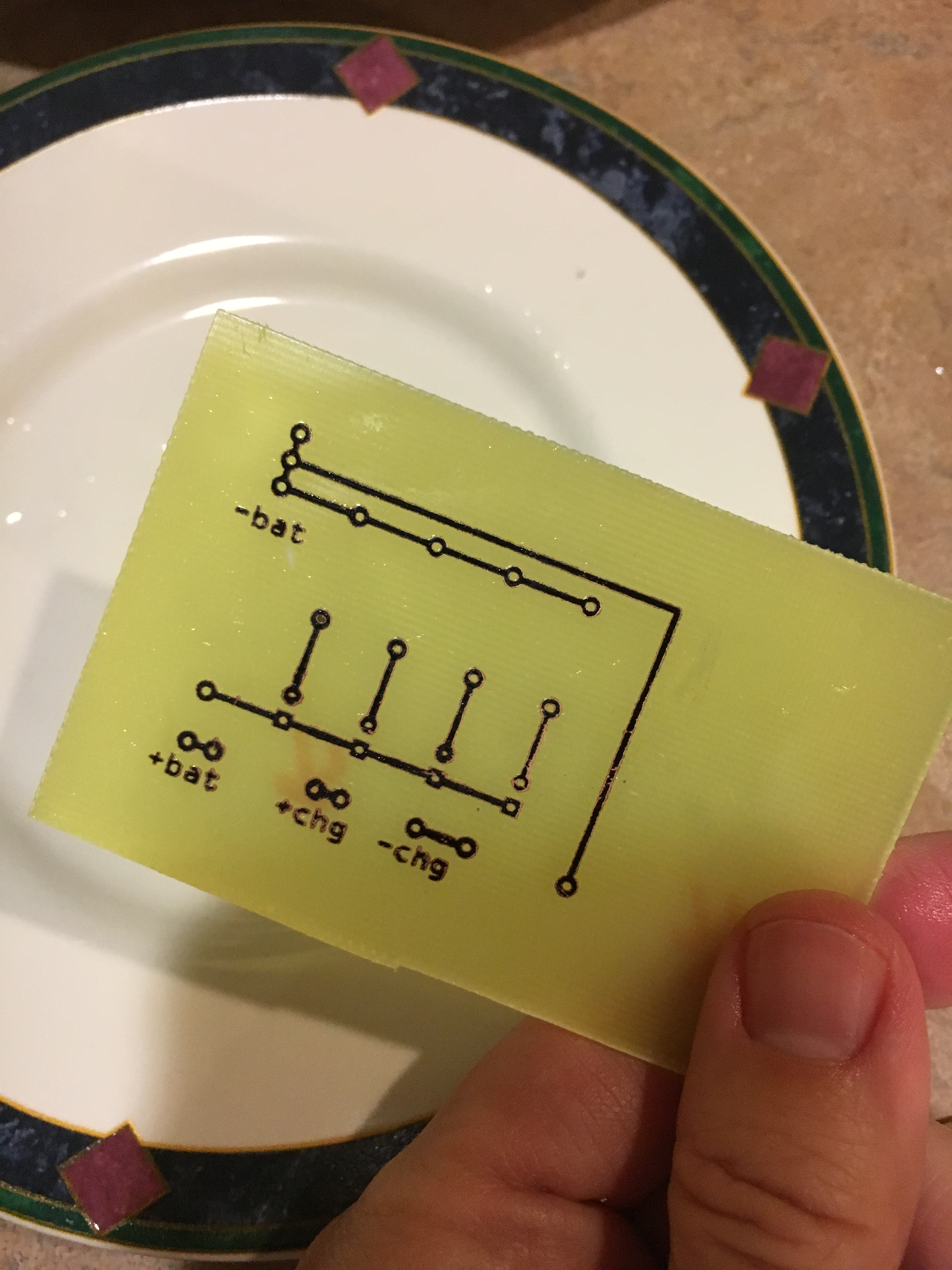
When the board was rinsed, we took paper towels and some nail polish remover (acetone) and scrubbed the rest of the toner off the board until the copper was visible.
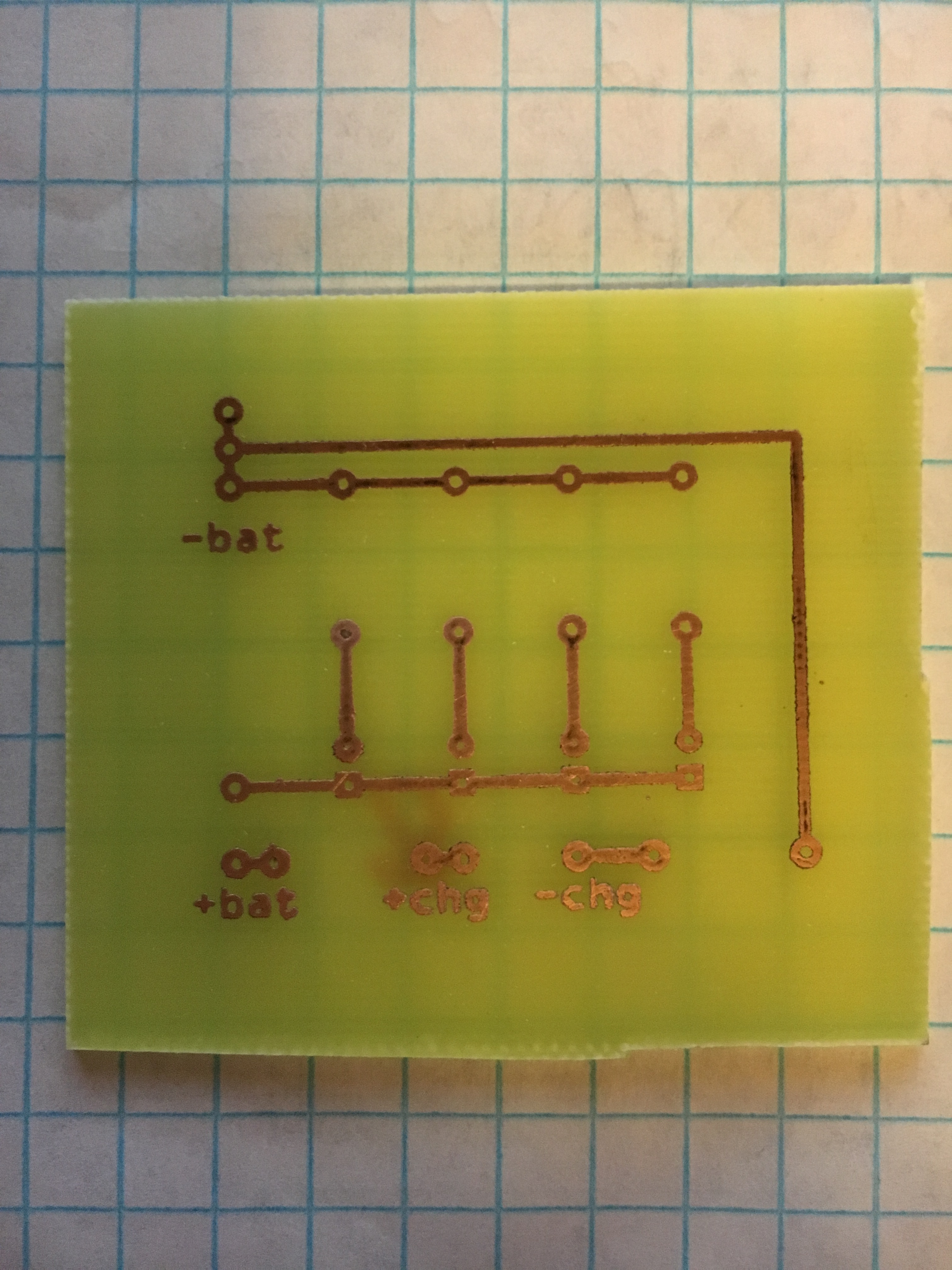
After scrubbing with acetone. Ready for drilling!
I used Blondihack’s method for drilling holes with a Dremel tool. I did the drilling and chose not to let students use the Dremel. It has the potential to really hurt you and this step requires a steady hand. Get your inner brain surgeon ready.
For the drilling, you’ll need:
- A Dremel rotary tool
- Quick-change Collet nuts (you need the smallest one) or a 1/32 inch drill chuck
- A 1/32 inch drill bit (I bought this set)
- A clamp and a piece of scrap wood
I recommend clamping your PCB to the table on top of scrap wood. You really want to make sure it doesn’t move around. Wear the safety goggles. Use the 1/32 inch drill bit and carefully drill a hole in each location on the PCB.
Next the students can solder the components onto the PCB. You can only solder them onto the copper trace, not onto the blank side of the board. Clip on the battery and test it out! Students sometimes had to use solder or jumper wires to fix locations where the copper traces were broken or thin. They cut the boards down to size with tin snips (fairly cheap at Home Depot) and sanded them when needed.
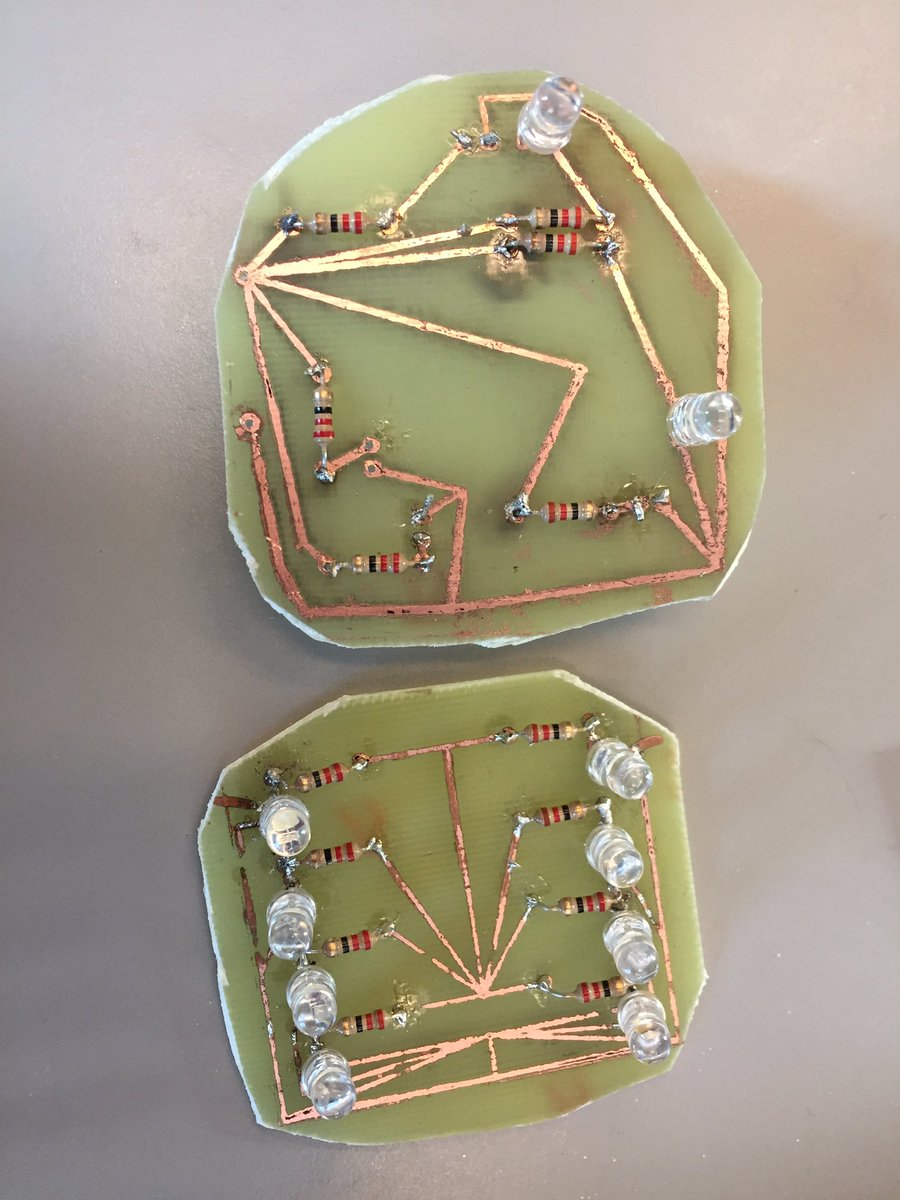
Soldered and cut! They look great.
The groups that had fewer problems were able to finish their circuit boards in 3 class periods, but some student groups took up to 6 class periods. These groups had to re-do steps along the way, usually in the printing and transferring, but sometimes in the soldering as well.
It was a supremely rewarding process. The students were so proud of their work. We all learned a lot about how printed circuit boards are made, and I think the kids felt as empowered as I did when I made my first PCB with that student so long ago. Students stayed after class and after school, trying over and over to get the process right. They really wanted to finish it once they started.
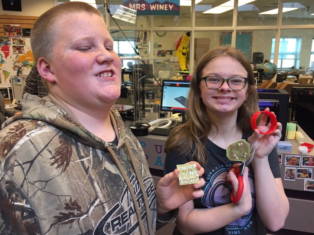
Showing off their work with pride!
I would strongly recommend having extra adult supervision if you try this activity with kids. Six students at a time seemed to be my capacity – consider bringing in parent volunteers or community members and training them on what to do. Plan ahead for science lab space, drilling and soldering, and for how you’re going to manage failures, because they will happen. It’s part of engineering.
If you try PCB etching with your engineering students, I’d love to hear from you. What went well? What would you do differently? What did I miss that I could be doing better?
Thanks a bunch to Quinn Dunki and Jason Rollette for their tutorials.

Recent Comments